Data Sheet
ADP2140
Rev. A | Page 25 of 32
capacitor is recommended to help minimize the input voltage
ripple. Use the following equation to determine the minimum
input capacitance:
IN
OUT
IN
OUT
MAX
LOAD
CIN
V
V
V
V
I
I
)
(
)
(
-
?/DIV>
EFFICIENCY
Efficiency is defined as the ratio of output power to input power.
The high efficiency of the ADP2140 has two distinct advantages.
First, only a small amount of power is lost in the dc-to-dc con-
verter package, which in turn, reduces thermal constraints. In
addition, high efficiency delivers the maximum output power
for the given input power, thereby extending battery life in
portable applications.
Power Switch Conduction Losses
Power switch dc conduction losses are caused by the flow of
output current through the P-channel power switch and the
N-channel synchronous rectifier, which have internal resis-
tances (R
DS(ON)
) associated with them. The amount of power
loss can be approximated by
2
_
)
(
_
)
(
_
))
1
(
(
OUT
N
ON
DS
P
ON
DS
COND
SW
I
D
R
D
R
P
?/DIV>
-
?/DIV>
+
?/DIV>
=
where
IN
OUT
V
V
D =
The internal resistance of the power switches increases with
temperature but decreases with higher input voltage.
Inductor Losses
Inductor conduction losses are caused by the flow of current
through the inductor, which has an internal resistance (DCR)
associated with it. Larger size inductors have smaller DCR,
which can decrease inductor conduction losses. Inductor core
losses relate to the magnetic permeability of the core material.
Because the ADP2140 is a high switching frequency dc-to-dc
converter, shielded ferrite core material is recommended for its
low core losses and low EMI.
To estimate the total amount of power lost in the inductor, use
the following equation:
PL = DCR ?/SPAN> IOUT
2
+ Core Losses
Switching Losses
Switching losses are associated with the current drawn by the
driver to turn on and turn off the power devices at the switching
frequency. Each time a power device gate is turned on and
turned off, the driver transfers a charge, 擰, from the input
supply to the gate, and then from the gate to ground.
Estimate switching losses using the following equation:
PSW = (CGATE_P + CGATE_N) ?/SPAN> VIN
2
?fSW
where:
C
GATE_P
is the gate capacitance of the internal high-side switch.
CGATE_N is the gate capacitance of the internal low-side switch.
fSW is the switching frequency.
Transition Losses
Transition losses occur because the P-channel switch cannot
turn on or turn off instantaneously. In the middle of an SW
node transition, the power switch provides all of the inductor
current. The source-to-drain voltage of the power switch is half
the input voltage, resulting in power loss. Transition losses
increase with both load current and input voltage and occur
twice for each switching cycle.
Use the following equation to estimate transition losses:
P
TRAN
= V
IN
/2 ?I
OUT
?(t
r
+ t
f
) ?f
SW
where:
t
r
is the rise time of the SW node.
t
f
is the fall time of the SW node.
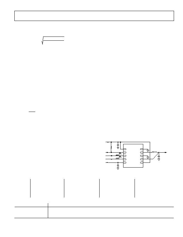
RECOMMENDED BUCK EXTERNAL COMPONENTS
The recommended buck external components for use with the
ADP2140 are listed in Table 8 (inductors) and Table 9 (capacitors).
VIN1
PGND
PG
SW
EN1
AGND
EN2
PG
EN1
EN2
FB
VOUT2
10
9
8
7
6
VIN2
1
2
3
4
5
ADP2140
100k&
+
CIN
10礔
+
COUT2
1礔
+
COUT
10礔
IN1
= 3.6
V
OUT2
= 1.8V
1礖
V
OUT
= 1.2
Figure 86. Typical Application Circuit with LDO Connected to Input Voltage
Table 8. 1.0 糎 Inductors
Vendor
Model
Case Size
Dimensions
ISAT (mA)
DCR (m?
Murata
LQM21PN1R0MC0D
0805
2.0 mm ?1.25 mm ?0.5 mm 800
190
Murata
LQM31PN1R0M00L
1206
3.2 mm ?1.6 mm ?0.95 mm 1200
120
Murata
LQM2HPN1R0MJ0
1008
2.5 mm ?2.0 mm ?0.95 mm 1500
90
FDK
MIPSA2520D1R0
2.5 mm ?2.0 mm ?1.0 mm
1200
90
Table 9. 10 糉 Capacitors
Vendor
Type
Model
Case Size
Voltage Rating
Murata
X5R
GRM219R60J106
0805
6.3 V
Taiyo Yuden
X5R
JMK212BJ106
0805
6.3 V
TDK
X5R
C1608X5R0J106
0603
6.3 V
发布紧急采购,3分钟左右您将得到回复。
相关PDF资料
ADP5022ACBZ-6-R7
IC REG TRPL BCK/LINEAR 16WLCSP
ADP5041ACPZ-1-R7
IC REG TRPL BCK/LINEAR 20-LFCSP
ADP5042ACPZ-2-R7
IC REG TRPL BCK/LINEAR 20LFCSP
ADT6402SRJZ-RL7
IC TEMP SENS TRIP PT PP SOT-23-6
ADT6501SRJZP085RL7
IC TEMP SENSOR MICROPWR SOT23-5
ADT7302ARTZ-500RL7
IC SENSOR TEMP 13BIT DGT SOT23-6
ADT7310TRZ
IC TEMP SENSOR 16BIT SPI 8SOIC
ADT7461AARMZ-R
IC TEMP SENSOR DGTL 2CH 8-MSOP
相关代理商/技术参数
ADP2140CPZ-REDYKIT
功能描述:REDYKIT 2 BOARDS ADP2140ACPZ RoHS:是 类别:编程器,开发系统 >> 评估板 - 线性稳压器 (LDO) 系列:* 产品变化通告:1Q2012 Discontinuation 30/Mar/2012 设计资源:NCP590MNDPTAGEVB Gerber Files 标准包装:1 系列:- 每 IC 通道数:2 - 双 输出电压:1.8V,2.8V 电流 - 输出:300mA 输入电压:2.1 ~ 5.5 V 稳压器类型:正,固定式 工作温度:-40°C ~ 85°C 板类型:完全填充 已供物品:板 已用 IC / 零件:NCP590MNDP 其它名称:NCP590MNDPTAGEVB-NDNCP590MNDPTAGEVBOS
ADP2147
制造商:AD 制造商全称:Analog Devices 功能描述:Compact, 800 mA, 3 MHz, Simple DVS, Buck Regulator Input voltage: 2.3 V to 5.5 V
ADP2147ACBZ-110-R7
功能描述:IC REG BUCK SYNC 0.8A 6WLCSP RoHS:是 类别:集成电路 (IC) >> PMIC - 稳压器 - DC DC 开关稳压器 系列:- 产品培训模块:High Efficiency Current Mode Switching Regulators
CMOS LDO Regulators 特色产品:BD91x Series Step-Down Regulators 标准包装:2,500 系列:- 类型:降压(降压) 输出类型:两者兼有 输出数:2 输出电压:3.3V,0.8 V ~ 2.5 V 输入电压:4.5 V ~ 5.5 V PWM 型:电流模式 频率 - 开关:1MHz 电流 - 输出:1.5A 同步整流器:是 工作温度:-40°C ~ 85°C 安装类型:表面贴装 封装/外壳:20-VFQFN 裸露焊盘 包装:带卷 (TR) 供应商设备封装:VQFN020V4040 产品目录页面:1373 (CN2011-ZH PDF) 其它名称:BD9152MUV-E2TR
ADP2147ACBZ-130-R7
功能描述:IC REG BUCK SYNC 0.8A 6WLCSP RoHS:是 类别:集成电路 (IC) >> PMIC - 稳压器 - DC DC 开关稳压器 系列:- 标准包装:500 系列:- 类型:切换式电容器(充电泵),反相 输出类型:固定 输出数:1 输出电压:-3V 输入电压:2.3 V ~ 5.5 V PWM 型:Burst Mode? 频率 - 开关:900kHz 电流 - 输出:100mA 同步整流器:无 工作温度:-40°C ~ 85°C 安装类型:表面贴装 封装/外壳:SOT-23-6 细型,TSOT-23-6 包装:带卷 (TR) 供应商设备封装:TSOT-23-6 其它名称:LTC1983ES6-3#TRMTR
ADP2147ACBZ-150-R7
功能描述:IC REG BUCK SYNC 1.2V/1V 6WLCSP RoHS:是 类别:集成电路 (IC) >> PMIC - 稳压器 - DC DC 开关稳压器 系列:- 标准包装:500 系列:- 类型:切换式电容器(充电泵),反相 输出类型:固定 输出数:1 输出电压:-3V 输入电压:2.3 V ~ 5.5 V PWM 型:Burst Mode? 频率 - 开关:900kHz 电流 - 输出:100mA 同步整流器:无 工作温度:-40°C ~ 85°C 安装类型:表面贴装 封装/外壳:SOT-23-6 细型,TSOT-23-6 包装:带卷 (TR) 供应商设备封装:TSOT-23-6 其它名称:LTC1983ES6-3#TRMTR
ADP2147ACBZ-170-R7
功能描述:IC REG BUCK SYNC 0.8A 6WLCSP RoHS:是 类别:集成电路 (IC) >> PMIC - 稳压器 - DC DC 开关稳压器 系列:- 标准包装:500 系列:- 类型:切换式电容器(充电泵),反相 输出类型:固定 输出数:1 输出电压:-3V 输入电压:2.3 V ~ 5.5 V PWM 型:Burst Mode? 频率 - 开关:900kHz 电流 - 输出:100mA 同步整流器:无 工作温度:-40°C ~ 85°C 安装类型:表面贴装 封装/外壳:SOT-23-6 细型,TSOT-23-6 包装:带卷 (TR) 供应商设备封装:TSOT-23-6 其它名称:LTC1983ES6-3#TRMTR
ADP2147CB-110EVALZ
功能描述:BOARD EVAL ADP2147ACBZ-110 RoHS:是 类别:编程器,开发系统 >> 评估板 - DC/DC 与 AC/DC(离线)SMPS 系列:* 产品培训模块:Obsolescence Mitigation Program 标准包装:1 系列:True Shutdown™ 主要目的:DC/DC,步升 输出及类型:1,非隔离 功率 - 输出:- 输出电压:- 电流 - 输出:1A 输入电压:2.5 V ~ 5.5 V 稳压器拓扑结构:升压 频率 - 开关:3MHz 板类型:完全填充 已供物品:板 已用 IC / 零件:MAX8969
ADP2147CB-130EVALZ
功能描述:BOARD EVAL ADP2147ACBZ-130 RoHS:是 类别:编程器,开发系统 >> 评估板 - DC/DC 与 AC/DC(离线)SMPS 系列:* 产品培训模块:Obsolescence Mitigation Program 标准包装:1 系列:True Shutdown™ 主要目的:DC/DC,步升 输出及类型:1,非隔离 功率 - 输出:- 输出电压:- 电流 - 输出:1A 输入电压:2.5 V ~ 5.5 V 稳压器拓扑结构:升压 频率 - 开关:3MHz 板类型:完全填充 已供物品:板 已用 IC / 零件:MAX8969